 11

An ambitious chip startup, Kepler Computing, has spent over seven years in quiet development, meticulously redesigning the fundamental architecture for computer memory. Now, having officially come out of stealth mode, the company is poised to revolutionize the semiconductor industry with a new approach that it believes can significantly ease the persistent global memory-chip shortage, provided its innovative technology can be produced at scale.
Founded in 2018 by a distinguished team of physicists and computer scientists, the San Jose, California-based startup asserts that its newly developed architecture for high-bandwidth memory (HBM) directly confronts and alleviates critical chip supply bottlenecks currently plaguing the global computing market. This breakthrough comes at a time when the demand for advanced memory is skyrocketing, particularly driven by the exponential growth of artificial intelligence and data center infrastructure.
Traditionally, chipmakers rely heavily on highly sophisticated and extraordinarily expensive extreme ultraviolet lithography (EUV) technology to shrink transistors, thereby packing an ever-increasing amount of processing power and memory into smaller physical footprints. Kepler Computing, however, claims a radically different path. Its proprietary "3D stacking" approach, coupled with the use of a novel, secret material, allows it to achieve significant density increases without any reliance on EUV. This is a monumental advantage, as it means Kepler’s technology can be integrated into existing semiconductor fabrication plants (fabs), circumventing the need for multi-billion-dollar investments in new, state-of-the-art EUV equipment and facilities.
The company’s advancements aren’t limited to HBM. Kepler also reports similar gains for high-speed cache memory, specifically Static Random-Access Memory (SRAM), which is typically embedded within the core of a chip die (such as CPUs, GPUs, and XPUs) to minimize data transfer times. While SRAM is critical for immediate data access, HBM, by contrast, utilizes stacks of Dynamic Random-Access Memory (DRAM) and functions as a separate, high-capacity memory component, crucial for handling massive datasets in AI and high-performance computing. Kepler’s ability to innovate in both these vital memory segments positions it uniquely in the market.
Kepler Computing has attracted substantial financial backing, having successfully raised $468 million in funding over the past few years from a roster of prominent investors. These include industry giants like GlobalFoundries, Intel Capital, and AMD Ventures, alongside major financial institutions such as the British investment fund Baillie Gifford, and even personal investment from Bill Gates through his private Gates Frontier fund. Further underscoring the strategic importance of Kepler’s work, the US Department of Commerce made a significant commitment in July. It announced an intention to provide Kepler with up to $245 million to foster the development of "a new class of high-performance AI memory technology, enabled by innovative 3D and ferroelectric technologies," specifically within the United States. This federal support highlights a national interest in bolstering domestic semiconductor manufacturing and innovation.
Currently, much of Kepler’s testing and initial production efforts are concentrated in Singapore, where its manufacturing partner and investor, GlobalFoundries, operates a major facility. GlobalFoundries has invested $50 million in Kepler, solidifying their partnership. Over the past two years, Kepler has been meticulously establishing what it refers to as "mini fabs" within GlobalFoundries’ existing infrastructure. In these specialized units, Kepler produces its advanced memory chips in conjunction with GlobalFoundries’ established 28-nanometer chip technology. Parallel testing and development have also been conducted at GlobalFoundries’ facilities in Burlington, Vermont, indicating a dual-pronged approach to development and potential future production.

Industry observers, along with Kepler and its investors, unanimously agree that the timing for the startup’s novel approach to building memory chips could not be more opportune. The persistent global memory chip shortage has starkly illuminated two enduring realities of the semiconductor market: firstly, constructing new fabrication plants is an immensely costly and time-consuming endeavor, often taking years and tens of billions of dollars; and secondly, the demand for specific types of memory tends to fluctuate cyclically, with current unprecedented demand centered on high-bandwidth memory. In an increasingly data-center-driven and AI-crazed world, HBM has unequivocally become the memory technology of choice, indispensable for the intensive computational requirements of modern applications.
Major global memory manufacturers, including giants like SK Hynix and Micron, have been engaged in a frantic race to construct multi-billion-dollar fabs. Their aim is to meet the surging demand for HBM, betting that even by the time these colossal facilities become operational, the industry’s appetite for high-bandwidth memory will remain insatiable.
Debo Olaosebikan, a cofounder and the chief executive officer of Kepler Computing, shed light on the company’s strategic shift. "For a long time our thinking was that we’d work on SRAM first and then follow up with DRAM and HBM," Olaosebikan explained. "But with the launch of ChatGPT [in 2022] and the explosion of demand for an HBM alternative, we started working on our HBM road map. Now we’re making SRAM and HBM in parallel." This adaptive strategy underscores Kepler’s responsiveness to market dynamics and the overwhelming surge in AI-driven memory requirements.
Srini Ananth, managing director at Intel Capital, one of Kepler’s key investors, echoed this sentiment regarding market-driven development. "We didn’t go in thinking that this would be a replacement for DRAM or a replacement for SRAM," Ananth noted. "We figured the market would dictate that, and now you’re seeing a demand for both." This perspective highlights the complementary nature of Kepler’s innovations, addressing diverse memory needs across the computing spectrum.
By completely bypassing the reliance on extreme ultraviolet lithography, Kepler Computing joins a select group of tech startups actively striving to circumvent one of the most significant and costly bottlenecks in modern semiconductor manufacturing. The startup boldly claims that it can produce SRAM with a density comparable to that achieved by cutting-edge 2-nanometer or 3-nanometer chips, all without the prohibitive investment in EUV technology. This represents a potentially disruptive paradigm shift in chip fabrication.
Ed Kaste, senior vice president of GlobalFoundries’ CMOS business, articulated his company’s enthusiasm for Kepler’s approach: "Kepler’s approach is at the sweet spot of our strategy. It’s a new materials system, with multigenerational scaling potential, without having to build entirely new systems in the fab or invest in very expensive lithography equipment." This endorsement from a major foundry partner underlines the practical and economic advantages of Kepler’s innovation.
Material Impact

Kepler Computing’s overarching value proposition is elegantly simple: the accelerated computing market should not be forced to endure protracted waits for brand-new memory fabs to be constructed simply to meet burgeoning demand. Instead, the company argues, innovative approaches to building memory within existing fabrication plants can dramatically increase supply and reduce lead times.
Their strategy is essentially twofold. Regarding improvements in HBM, Kepler asserts it has developed a novel 3D-manufacturing technique. This method allows for the packing of more memory chips within an identical physical footprint, thereby increasing density and capacity. A crucial benefit of this technique is that the core compute unit can be positioned closer to the memory, significantly reducing the energy required for data transfer between the two components. Kepler’s ambitious ultimate goal is to enable data movement within HBM with energy efficiency comparable to SRAM, all while preserving HBM’s inherently large capacity. This would represent a major leap in both performance and power consumption.
Furthermore, Kepler has substantially improved the density of SRAM through the strategic use of ferroelectrics. Ferroelectric materials possess unique properties that enable them to read and write data at significantly lower voltages compared to the conventional mechanisms employed for data processing and storage in semiconductors. The startup achieved this by developing a groundbreaking, low-voltage, composite material that is optimized for this ferroelectric approach.
Sasi Manipatruni, a cofounder and Kepler’s chief technology officer, elaborated on the rigorous development process. He revealed that the Kepler team meticulously iterated through 35 different composite formulations before successfully identifying a material class that they believed would make memory chips both easier and more cost-effective to manufacture. "Once we found a way to solve the physics problem—as in the physical limitations for HBM—we came up with a material innovation that helps with the amount of memory you can have between chips," Manipatruni stated, highlighting the dual challenge of fundamental physics and material science they overcame.
In its initial collaborative build-outs with GlobalFoundries, Kepler proudly reports an impressive feat: they were able to convert an existing fab into a "next-generation" facility capable of their advanced manufacturing processes in a mere eight months. This stands in stark contrast to the typical 24-month timeframe usually required for such significant upgrades or new fab constructions.
"Our goal is to take the fabs and architectures already built, and push them to the limits of physics," Olaosebikan affirmed, encapsulating the company’s core philosophy. Essentially, Kepler is making a compelling wager: any additional costs incurred from developing new materials or retooling existing fabs will be vastly outweighed by the staggering $20 billion to $40 billion price tag associated with constructing entirely new fabrication plants and outfitting them with equipment worth hundreds of millions of dollars each.
Waiting to Scale

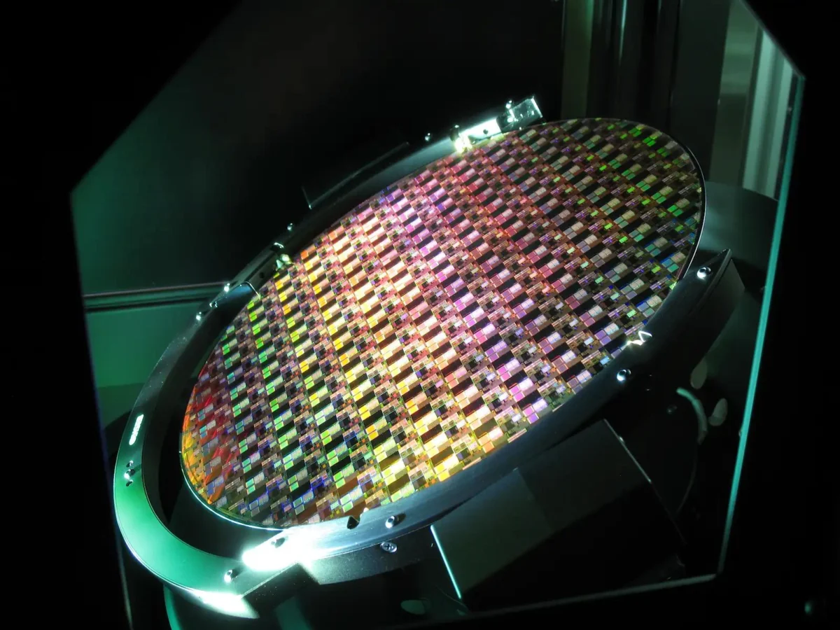
Despite its groundbreaking innovations and significant financial backing, Kepler Computing still faces a formidable journey before it can achieve full-scale production – assuming it reaches that ambitious milestone. To date, the company has run its technology on approximately 2,000 wafers, a critical but still relatively small number in the vast landscape of semiconductor manufacturing. The startup has outlined an aggressive timeline: it plans to ship its initial samples of HBM chips later this year, intends to ramp up production from its Singapore facilities next year, and aims to commence chip production within the United States by 2028.
Ed Kaste of GlobalFoundries expressed a cautious optimism, stating his confidence that the "fundamental breakthroughs have happened. What remains is getting good results on thousands of wafers and millions of devices." This sentiment underscores the inherent challenge in semiconductor manufacturing: proving a concept is one thing, but consistently producing millions of flawless devices at scale is an entirely different, and far more complex, undertaking.
Kaste also highlighted a specific technical hurdle associated with Kepler’s material system: the inclusion of iron in its composite. "Iron is a tough contaminant to introduce into a production facility," he explained. "So Kepler’s solution has to run on dedicated equipment, or be fully encapsulated so that it can’t escape." This necessity demands stringent control measures to prevent cross-contamination in shared fab environments, adding a layer of complexity to the manufacturing process. "The art is in keeping that material really well isolated through our production flow," Kaste emphasized, pointing to the meticulous engineering required.
Olaosebikan, while acknowledging the proprietary nature of their innovation, remained discreet about the specific elements of the company’s composite material. "What I can say is, we’re using a small number of materials, and some of them aren’t what you’d typically find in mainstream ferroelectrics," he offered, hinting at the unique chemical makeup of their breakthrough.
Kepler Computing is not an isolated phenomenon in its quest to disrupt the entrenched semiconductor industry. Late last year, another well-funded startup named Substrate also garnered significant attention for its novel approach to lithography, utilizing nanoparticles to etch intricate details onto advanced chips. However, some industry analysts expressed skepticism regarding Substrate’s ambitious claims, noting the extreme difficulty of producing a large volume of chips "that meet incredibly stringent specifications, on time and on budget," as reported by Bloomberg.
The challenge of scaling production is a pervasive obstacle when attempting to introduce radical innovations in semiconductor manufacturing, whether these involve entirely new processes, materials, or a combination of both. Austin Lyons, a chip analyst for Creative Strategies, who was not privy to Kepler’s specific innovations, articulated this common dilemma: "The question is how to overcome all the limitations of contamination, different materials, and different tooling, in such a way that the resulting innovation can be used at scale and is worth the cost."
Ultimately, while proving the efficacy of a new method for memory production is a significant achievement, the monumental task of meeting the historic and ever-growing demand for it at a global scale will be Kepler Computing’s ultimate test. Their success hinges not just on innovation, but on robust execution and flawless industrialization.